
Balanced Modulators
General Description The LM1596/LM1496 are doubled balanced modulator-de- modulators which produce an output voltage proportional to the product of an input (signal) voltage and a switching (car- rier) signal.
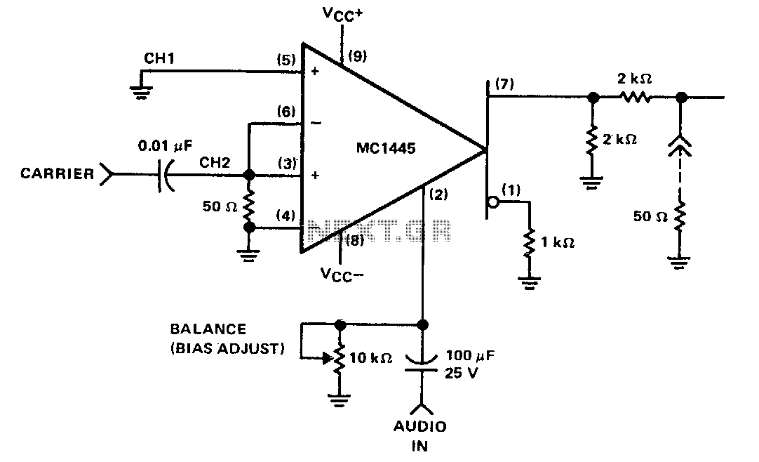
video modulator circuit Video Circuits Next.gr
Balanced Modulators/ Demodulators These devices were designed for use where the output voltage is a product of an input voltage (signal) and a switching function (carrier). Typical applications include suppressed carrier and amplitude modulation, synchronous detection, FM detection, phase detection, and chopper applications.
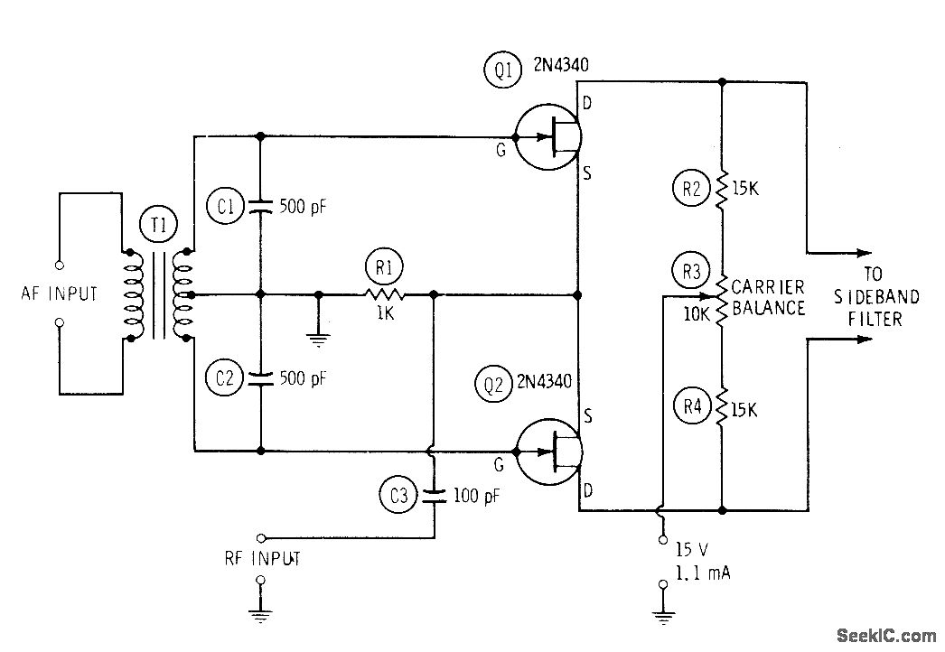
FET BALANCED MODULATOR FOR SSB under Repositorycircuits 53908 Next.gr
Balanced Modulation. Ring or Balanced Modulation is technically known as four-quadrant modulation as it always produces sound, regardless of whether the modulator or the carrier are negative or positive. In addition to the two quadrants described above for amplitude modulation, when the modulator is negative, the positive and negative.
PPT Figure 41 Balanced ring modulator. PowerPoint Presentation, free
any hybrid or IC balanced modulator/demodulator and is comparable to that of costly signal processing instruments. 3. The op amp format of the AD630 ensures easy implementation of high gain or complex switched feedback functions. The application resistors facilitate the implementation of most common applications with no additional parts. 4.
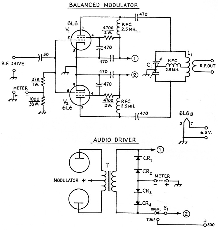
Highlevel balanced modulator for D.S.B.
4-4 Balanced Modulators Modulation 4-5 SSB Circuits Chapter Objectives. Explain the relationship of the basic equation for an AM signal to the production of amplitude modulation, mixing, and frequency conversion by a diode or other nonlinear frequency component or circuit.. Describe the operation of diode modulator circuits and diode.

Balanced Modulator FET circuit Suppression of Carrier DSBSC
Balanced modulator consists of two identical AM modulators. These two modulators are arranged in a balanced configuration in order to suppress the carrier signal. Hence, it is called as Balanced modulator. The same carrier signal c(t) = Ac cos(2πfct) c ( t) = A c cos ( 2 π f c t) is applied as one of the inputs to these two AM modulators.

(a) Balanced BPSK modulator circuit, (b) S 21 of the modulator using
A Balanced Modulator Circuit is a type of modulator that produces an output signal that is the product of two input signals- the message signal and the carrier signal. Balanced Modulator Circuit consists of two or more active devices circuit arranged in a balanced fashion so as to suppress the carrier signal.

Balanced Modulators
Learn more about this topic in Chapter 25 of.http://www.amazon.com/Teach-Yourself-Electricity-Electronics-5th/dp/0071741356/
More components are installed on the balanced modulator board.
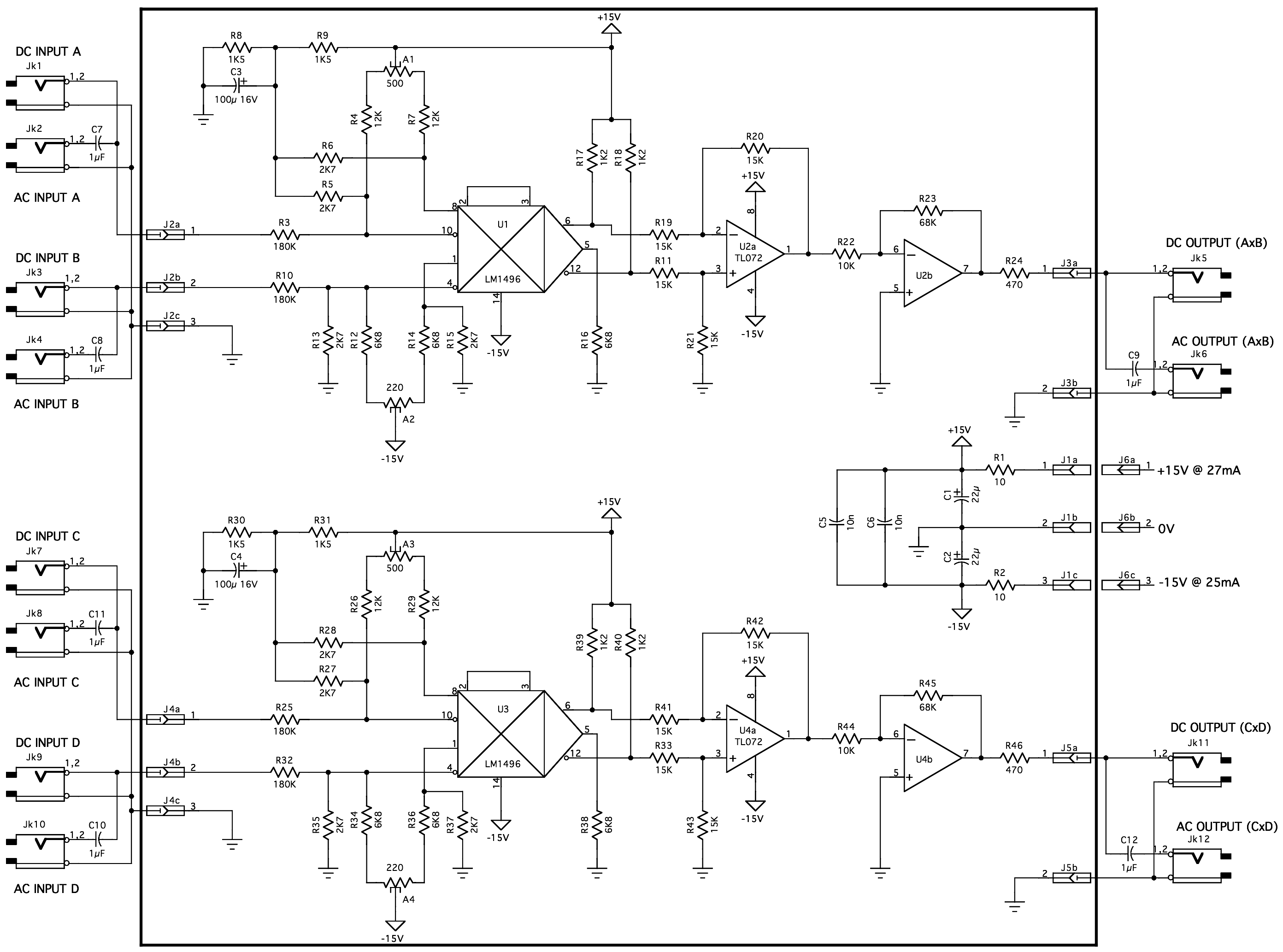
Download scientific diagram | Balanced Modulator-Demodulator typical Circuit. from publication: Quadrature Phase Shift Keying modulator & demodulator for Wireless Modem | Digital modulation is a.
100_KC_HYBRID_BALANCED_MODULATOR Signal_Processing Circuit Diagram
Balanced Modulators/ Demodulators These devices were designed for use where the output voltage is a product of an input voltage (signal) and a switching function (carrier). Typical applications include suppressed carrier and amplitude modulation, synchronous detection, FM detection, phase detection, and chopper applications.

Diode Modulators, April 1953 QST RF Cafe
Modulators (sometimes called balanced-modulators, doubly-balanced modulators or even on occasions high level mixers) can be viewed as sign-changers. The two inputs, X and Y, generate an output W, which is simply one of these inputs (say, Y) multiplied by just the sign of the other (say, X), that is W = Ysign(X).
Balanced_modulator_for_SSB_operation Electrical_Equipment_Circuit
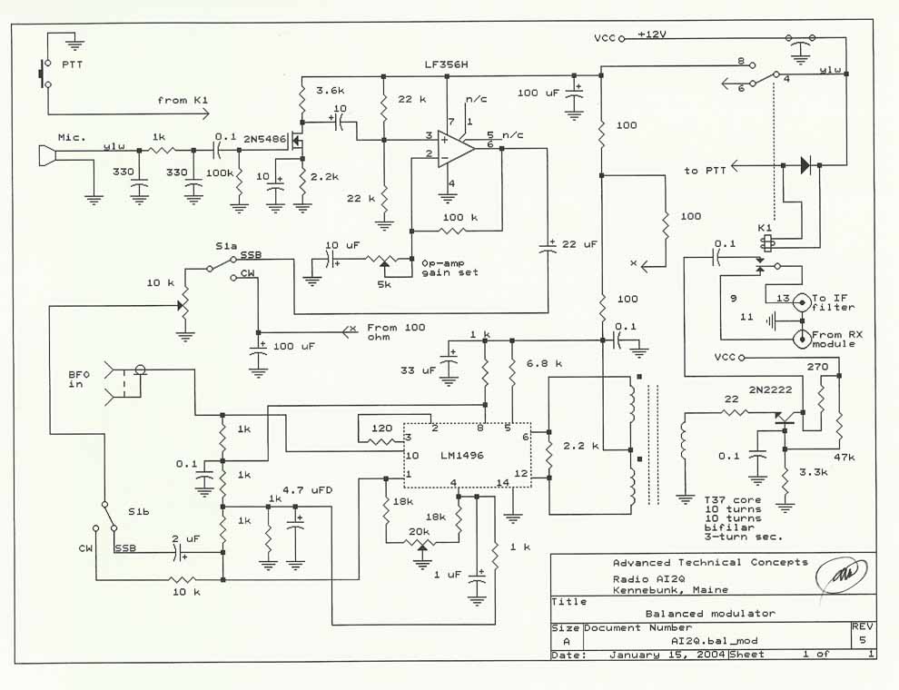
(G7C01) A balanced modulator is the circuit used to combine signals from the carrier oscillator and speech amplifier and send the result to the filter in a typical single-sideband phone transmitter. (G7C02)
PPT Figure 41 Balanced ring modulator. PowerPoint Presentation, free
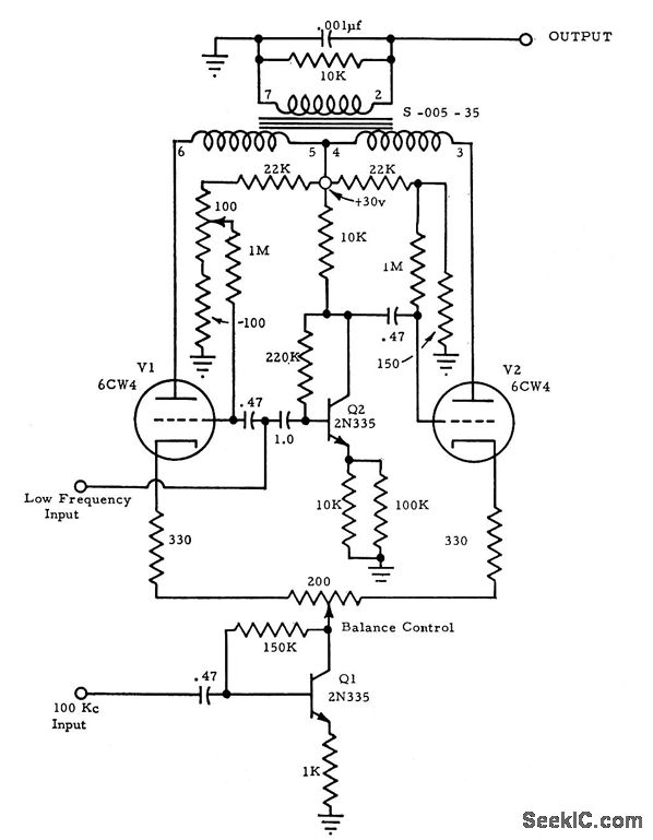
Two balanced modulator circuits using diodes and transistors as nonlinear devices are shown in Figs. 22.33 (a) and 22.33 (b). It is assumed that both diodes and transistors used in circuits shown in Fig. 22.33 have identical characteristics and that the circuit is symmetrical with respect to the centre tap of the transformer. As the two halves.
Circuit Diagram Of Balanced Modulator
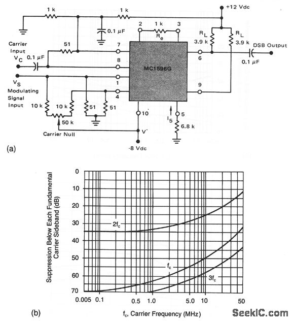
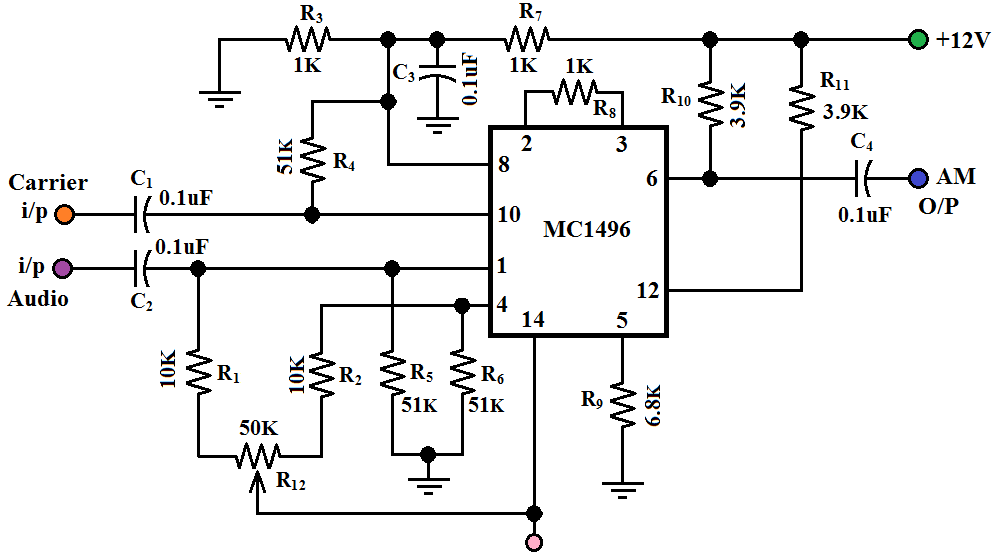
The MC1496 is a monolithic transistor array arranged as a balanced modulator-demodulator. The device takes advantage of the excellent matching qualities of monolithic devices to provide superior carrier and signal rejection. Carrier suppressions of 50dB at 10MHz are typical with no external balancing networks required.
index.thml
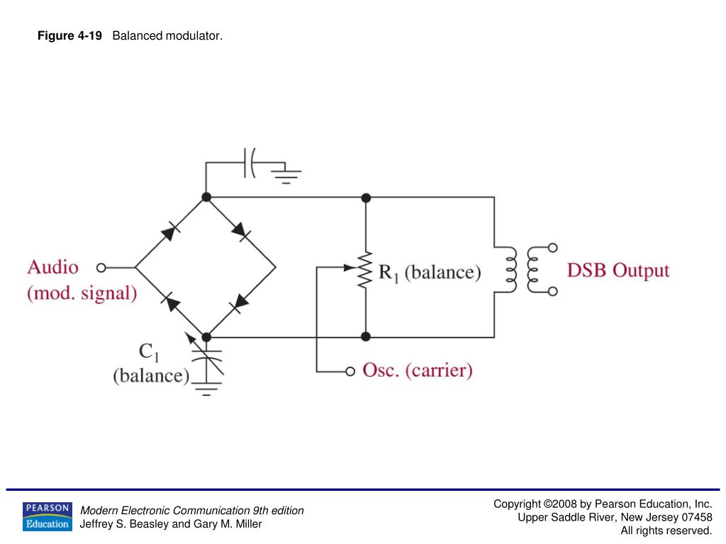
Therefore, a balanced modulator may be defined as a circuit in which two non-linear devices are connected in a balanced mode to produce a DSB-SC signal . In this article, we shall discuss a balanced modulator circuit using diodes . Fig.1 shows the balanced modulator using diodes as non-linear device . Fig 1

Balanced Modulators
4.1 MC1496 Balanced Modulator/Demodulator The MC1496 is a monolithic transistor array integrated circuit (IC) arranged as a balanced modula-tor/demodulator. It was designed for use where the output voltage is a product of an input voltage (the message) and a switching function (the carrier). Typical applications include double-sideband